- 您现在的位置:买卖IC网 > Sheet目录3873 > PIC18F13K50-I/P (Microchip Technology)IC PIC MCU FLASH 4KX16 20-PDIP
dsPIC30F1010
/202X
DS7
0178C-page
218
P
reli
m
inary
20
06
M
ic
rochip
T
e
c
hnology
In
c
.
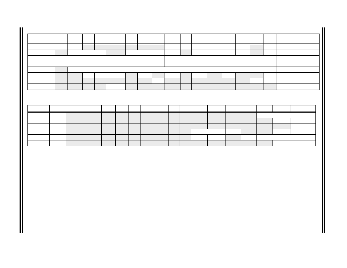
TABLE 18-8:
SYSTEM INTEGRATION REGISTER MAP FOR dsPIC30F202X
SFR
Name
Addr
.
Bit 15
Bit 14
Bit 13
Bit 12
Bit 11
Bit 10
Bit 9
Bit 8
Bit 7
Bit 6
Bit 5
Bit 4
Bit 3
Bit 2
Bit 1
Bit 0
Reset State
RCON
0740
TRAPR
IOPUWR
—
EXTR
SWR
SWDTEN
WDTO
SLEEP
IDLE
—
POR
Depends on type of Reset.
OSCCON
0742
—
COSC<2:0>
—
NOSC<2:0>
CLKLOCK
—
LOCK
PRCDEN
CF
TSEQEN
—
OSWEN Depends on Configuration bits.
OSCTUN
0748
TSEQ3<3:0>
TSEQ2<3:0>
TSEQ1<3:0>
TUN<3:0>
0000 0000 0000 0000
OSCTUN2
074A
TSEQ7<3:0>
TSEQ6<3:0>
TSEQ5<3:0>
TSEQ4<3:0>
0000 0000 0000 0000
LFSR
074C
—
LFSR<14:0>
0000 0000 0000 0000
PMD1
0770
—
—T3MD
T2MD
T1MD
—
PWMMD
—I2CMD
—U1MD
—
SPI1MD
—
—ADCMD
0000 0000 0000 0000
PMD2
0772
—
—IC1MD
—
—OC2MD
OC1MD
0000 0000 0000 0000
PMD3
0774
—
CMP_PSMD
—
0000 0000 0000 0000
Note:
Refer to the “dsPIC30F Family Reference Manual” (DS70046) for descriptions of register bit fields.
TABLE 18-9:
DEVICE CONFIGURATION REGISTER MAP
File Name
Addr.
Bits 23-16
Bit 15
Bit 14
Bit 13
Bit 12
Bit 11
Bit 10
Bit 9
Bit 8
Bit 7
Bit 6
Bit 5
Bit 4
Bit 3
Bit 2
Bit 1
Bit 0
FBS
F80000
—
BSS<2:0>
BWRP
FGS
F80004
—
GSS1
GSS0
GWRP
FOSCSEL
F80006
—
—FNOSC<1:0>
FOSC
F80008
—
FCKSM<1:0>
FRANGE
—
OSCIOFNC
POSCMD<1:0>
FWDT
F8000A
—
FWDTEN
WWDTEN
—
WDTPRE
WDTPOST<3:0>
FPOR
F8000C
—
—FPWRT<2:0>
Note:
Refer to the “dsPIC30F Family Reference Manual” (DS70046) for descriptions of register bit fields.
发布紧急采购,3分钟左右您将得到回复。
相关PDF资料
PIC16CR76T-I/SO
IC PIC MCU 8KX14 28SOIC
PIC18LF24K22-I/MV
IC PIC MCU 16KB FLASH 28UQFN
PIC18LF24K22-I/ML
IC PIC MCU 16KB FLASH 28QFN
PIC16CR76T-I/ML
IC PIC MCU 8KX14 28QFN
PIC16F627-04/P
IC MCU FLASH 1KX14 COMP 18DIP
PIC18F45J10-I/ML
IC PIC MCU FLASH 16KX16 44QFN
PIC18F24K22-I/ML
IC PIC MCU 16KB FLASH 28QFN
PIC16CR76-I/SS
IC PIC MCU 8KX14 28SSOP
相关代理商/技术参数
PIC18F13K50-I/P
制造商:Microchip Technology Inc 功能描述:20 Pin 8 KB Flash 512 RAM 15 I/O 10
PIC18F13K50-I/SO
功能描述:8位微控制器 -MCU 8KB Flash 512 RAM 15 I/O 10-B ADC USB 2.0 RoHS:否 制造商:Silicon Labs 核心:8051 处理器系列:C8051F39x 数据总线宽度:8 bit 最大时钟频率:50 MHz 程序存储器大小:16 KB 数据 RAM 大小:1 KB 片上 ADC:Yes 工作电源电压:1.8 V to 3.6 V 工作温度范围:- 40 C to + 105 C 封装 / 箱体:QFN-20 安装风格:SMD/SMT
PIC18F13K50-I/SO
制造商:Microchip Technology Inc 功能描述:20 Pin 8 KB Flash 512 RAM 15 I/O 10
PIC18F13K50-I/SS
功能描述:8位微控制器 -MCU 8KB Flash 512 RAM 15 I/O 10-B ADC USB 2.0 RoHS:否 制造商:Silicon Labs 核心:8051 处理器系列:C8051F39x 数据总线宽度:8 bit 最大时钟频率:50 MHz 程序存储器大小:16 KB 数据 RAM 大小:1 KB 片上 ADC:Yes 工作电源电压:1.8 V to 3.6 V 工作温度范围:- 40 C to + 105 C 封装 / 箱体:QFN-20 安装风格:SMD/SMT
PIC18F13K50-I/SS
制造商:Microchip Technology Inc 功能描述:8-Bit Microcontroller IC
PIC18F13K50T-I/SO
功能描述:8位微控制器 -MCU 8KB Flash 512 RAM 15 I/O 10-B ADC USB 2.0 RoHS:否 制造商:Silicon Labs 核心:8051 处理器系列:C8051F39x 数据总线宽度:8 bit 最大时钟频率:50 MHz 程序存储器大小:16 KB 数据 RAM 大小:1 KB 片上 ADC:Yes 工作电源电压:1.8 V to 3.6 V 工作温度范围:- 40 C to + 105 C 封装 / 箱体:QFN-20 安装风格:SMD/SMT
PIC18F13K50T-I/SS
功能描述:8位微控制器 -MCU 8KB Flash 512 RAM 15 I/O 10-B ADC USB 2.0 RoHS:否 制造商:Silicon Labs 核心:8051 处理器系列:C8051F39x 数据总线宽度:8 bit 最大时钟频率:50 MHz 程序存储器大小:16 KB 数据 RAM 大小:1 KB 片上 ADC:Yes 工作电源电压:1.8 V to 3.6 V 工作温度范围:- 40 C to + 105 C 封装 / 箱体:QFN-20 安装风格:SMD/SMT
PIC18F14K22-E/ML
功能描述:8位微控制器 -MCU 16KBFlash 512byteRAM 256bytesEEPROM
RoHS:否 制造商:Silicon Labs 核心:8051 处理器系列:C8051F39x 数据总线宽度:8 bit 最大时钟频率:50 MHz 程序存储器大小:16 KB 数据 RAM 大小:1 KB 片上 ADC:Yes 工作电源电压:1.8 V to 3.6 V 工作温度范围:- 40 C to + 105 C 封装 / 箱体:QFN-20 安装风格:SMD/SMT